Showing posts with label electronics. Show all posts

Syllabus Electronics nepal Electricity Authority ,NEA level 7


मिति 2014,08,09
g]kfn ljB"t\ k|flws/)f
k|fljlws ;]jf, On]lS^«sn ;d'x, On]S^«f]lgS; pk;d'x, tx-7 O{lGhlgo/ kbsf]
v"Nnf k|ltof]lutfTds lnlvt k/LIffsf] kf&\oqmd

1=    z}lIfs of]UotfM k|rlnt sd{rf/L ;]jf ljlgodfjnLdf Joj:yf eP cg";f/ .
2=    lnlvt k/LIffsf] ljifo, k')f{f+°, k/LIff k|)ffnL, k|Zg;+Vof, c+sef/ / ;do lgDgfg";f/ x"g]% .
kq
Ljifo
k')f{f+°
k/LIff k|)ffnL
k|Zg ;+Vof
k|lt k|Zg c+sef/
;do
k|yd
On]S^«f]lgS; O{lGhlgol/+é (I)
30
j:t"ut jx" pQ/
30
1
30 ldg]^
låtLo
On]S^«f]lgS; O{lGhlgol/+é (II)
70
ljifout
%f]^f] pQ/
8
5
2 #)^f 30 ldg]^
nfdf] pQ/
3
10

3=    a:t"ut jx"pQ/ k/LIff k|)ffnLdf k|To]s k|Zgsf rf/ j^f ;DefJo pQ/ lbOg] % . h; dWo] Pp^f ;xL pQ/df - √ _ lrGx nufpg" kg]{% .
4=   k|ydkq / låtLokqsf] k/LIff 2 k^s u/]/ x"g]% . k|ydkqsf] k/LIff ;lsP kl% låtLokqsf] k/LIff tTsfn x"g]% .

k|ydkq / låtLokqsf] kf&\oqmd ljj/)f

1.           Electric Circuits and Semiconductor devices
Electric Circuits: Circuit elements; series and parallel circuits; Kirchoff’s laws; Single phase and 3 phase circuits; Power and energy in AC circuits; Transfer functions; Frequency response of networks; Fourier series Transient and Steady state response
Semiconductor Materials: Intrinsic & extrinsic semiconductor; impurities, doping, p & n type semiconductor; majority and minority charge carriers, theory of PN junction
Semiconductor Devices: Diodes (PN junction diode, zener diode, LED, photo diode, tunnel diode, varactor diode, Schottky diode); Bipolar Transistor (Construction, Operations, Transistor configurations – CE, CB and CC Configurations; small signal model around a dc operating point, Transistor modeling; Different biasing and small signal analysis, BJT Frequency response); Field Effect Transistor (Construction, Characteristics, Types of FET, Basic FET circuits), Switching Circuits (TTL Circuits; MOSFET switch; NMOS Circuits; CMOS Circuits)

2.            Logic Circuits and Digital Electronics
Number System: Decimal, binary, octal, hexadecimal and BCD numbering systems, and their conversions
Logic Gates: NOT, OR, AND, NOR, NAND, X-OR, X-NOR gates, laws and theorems of Boolean algebra, K-map
Combinational Logics: Half Adder, Full Adder, N-bit adder, Encoder, Decoder, Multiplexer, Demultiplexer, ROM, PLA
Sequential Logics: Flip Flops, Shift Registers, Counter, Astable, Monostable and Bistable Multivibrator and Clock 
Digital Electronics: Bipolar Transistor Switching Characteristics; MOS Transistor Switching Characteristics; Bipolar Transistor Logic Circuits; NMOS Family of Logic Circuits; CMOS Family of Logic Circuits; Memory; Logic Gates

3.           Electronics Circuits
Operational Amplifier: OpAmps characteristics, Basic OpAmp circuits
Amplifiers: Class A, Class B, Class AB, Class C and Class D Amplifiers and their circuits; Classifications of Amplifiers on the basis of coupling – RF, Transformer, Direct Coupling Amplifier; Classifications of Amplifiers on the basis of Frequency – Audio, RF and Tuned Amplifiers
Oscillators: Feedback concepts, Oscillation theory; Relaxation oscillator; Colpitts, Hartley, Wien bridge, LC, Crystal Oscillators; Voltage Controlled Oscillator
Voltage Regulators and Power Supplies: Unregulated and regulated power supplies, voltage regulation, voltage reference, heat and power design, regulator ICs

4.           Communication system
Analog Communication: Modulation, theory and generation of AM, DSB-SC, SSB, FM and PM; comparison between AM, FM and PM; AM, FM and PM transmitters/receivers; superheterodyne receiver; IF & RF amplifiers, automatic gain control (AGC), balanced slope detector, phase discriminator, ratio detector, FM stereo principle, equalizers, noise in analog communication systems
Digital Communication: Advantages of digital communication; principle of PAM, PWM, PPM and PCM; OOK, PSK, DPSK, Four Phase PSK, FSK and QAM techniques; noise in digital communication systems
Optical Fibre Communication: Advantages of optical transmission, optical spectrum, types of optical fibre cable, attenuation in optical fibre cable, joining of fibres-mechanical coupling and fusion splicing, laser diodes, photodiodes, attenuation measurements, operation and line supervision, optical fibre network in NEA
Power Line Carrier Communication (PLCC): Introduction and general theory, transmission channels, frequency range, modulation technique, carrier frequency generation, transmitting amplifier, pilot channel, demodulation, HF filter tuning, line equalization, PLCC system in NEA
Microwave Communication: Microwave transmission and reception, microwave triodes, clystrons, magnetrons

5.           Electromagnetic Fields, Transmission Lines and Antennas
Electromagnetic Fields: Electrostatic Fields in Free Space; Gauss’s Law in Integral Form and Application (Conductors, insulators and semiconductors); Wave Equations (Polarization, wave impedance, skin effect, Reflection and refraction at the interface between two media, Standing wave ratio, Impedance matching, Quarter wave transformer)
Transmission Lines: Basic principles, fundamentals of transmission lines, characteristics impendence, Types of Transmission Lines (Coaxial cable, Open wire, Wave guide), Equivalent diagram of T.L., Matched and Mismatched T.L., losses in transmission lines, standing waves, Power and signal transmission capability of lines
Waveguides and Resonators: Theory and operation of waveguide, parallel plane, rectangular, circular, ridged and flexible waveguides; waveguide coupling, matching and attenuation; theory and operation of resonator
Antennas: Types, antenna gain, antenna resistance, bandwidth, beamwidth, polarization, directivity, effect of antenna height, dipole, dipole arrays, folded dipole; yagi, parabolic, horn, helical, discone and loop antannas, Propagation in the radio frequency spectrum

6.           Microprocessor and Microcomputer
Microprocessor: Registers, memory, and input/output, fundamental bus signals
Assembly Language Programming: Assembler syntax, macro assemblers, cross assembler
Internal Architecture of Basic Microprocessor: Internal resources of microprocessor – registers, data paths, control units and arithmetic and logic units, relation between RTL and assembly language
Interrupt Operations: Interrupt behavior, interrupt service routine requirements, interrupt priority, vectored, chained and polled interrupt structures, peripheral devices using interrupts
Microcomputer: Building blocks of a microcomputer, RISC and CISC computers, Operating systems, Software system concepts, Data communications concepts

7.           Instrumentation and Control
Applied Electronics: Voltage Summing, Voltage buffer; Switched Mode Power Supply; Inverters; Choppers; Diode, Thyristors, Triac, Controlled Rectifier Circuits; Darlington Pair, Wave Shaping Circuits; Active filters; Phase Lock Loops
Instrumentation: Instrumentation Systems; Theory of Measurements (Static performance – accuracy, precision, sensitivity, resolution and linearity; Dynamic Performance – response time, frequency response, bandwidth and errors in the measurements)
Measurement Transducers: Temperature, light level, strain and displacement, acceleration, pressure, force, velocity, magnetic field measurement
Digital to Analog Conversions: A/D and D/A conversions
Output Devices: Indicators, meters, strip chart recorder, magnetic tape recorders
Component Modeling and Linearization: Differential equations and transfer functions, state space formulation, fluid, fluidic and thermal system components, linearized approximation of non-linear characteristics
System Transfer Functions and Responses: Combinations of components to physical systems, system reductions, laplace transform, steady state equilibrium system,
Stability: characteristic equation, complex plane interpretation of stability, root locations and stability, Root Locus Method; Frequency Response Method; Performance Specifications for Control System

8.           Engineering Economics and Financial Analysis
Essential Business and Accounting Terminology: Cost Classification and Analysis; Interest and Time Value of Money; Demand Analysis and Sales Forecasting Tariff Structure; Methods of Economic/Financial Analysis; Investment Decision; Interest and Time value of Money
Basic Methodology of Engineering Economics Studies: Cost Benefit Analysis, Risk Analysis, Investment Decision, Internal Rate of Return, Net Present Worth, Payback Period

9.           Electronic Construction and Safety Engineering
Prototyping methods: Breadboards, PC prototyping boards
Printed Circuits: PC board fabrication, PC board designs, CAD/CAM
Safety and Precautions: Safety Rules and Regulations; Storage and handling of Explosives, Compressed Gases and Flammable Substances; Safety and Precautions in case of Hazards
Earthing and Shielding Techniques: Fire Hazards, Fire Fighting Techniques and Equipment
Noise Hazards: Sources of Noise, Control of Noise and its Effect on Health, First Aid Requirements for after the event treatment

10.              Institutional Know-How

(a)    General knowledge of Nepal Electricity Authority, its organizational structure and function of various business groups.
(b)   General knowledge of various power plants of Nepal, their types, salient features and their geographical locations.
(c)    General knowledge on Nepalese Power Transmission System, Voltage levels and Lengths, export-import links for Power exchange with India.

·

Wireless.Optical.Communication.Systems.Springer.Verlag.Telos

About us
We provide free e-books for download without any registration or money.
Search for any ebook you need in our search box.
Website:engineeringfourum.blogspot.com
Type:Free
Registration: no any
No of ebooks: 7037(total in this blog)
About book
Name : Wireless.Optical.Communication.Systems 
Author: 
Edition: 
Published on:2013-03-16 
File Format: 
Download link: Below
Description:The ebook s the wireless optical communication system.A free download book 
in our web .Search more ebook on our blog to download .
 Size:7MB
Image: 
 
Download Here
 Wireless.Optical.Communication.Systems.Springer.Verlag.Telos.pdf 

Electronics Ebooks TU Free download in PDF


electronic devices and circuit theory 9th edition pdf
                                                                  Download link here
Thomas l. Floud ,Electronics device , 8 th edition Pearson Education INC 2007

                                                                 Download link here
Mark N Horenstein  ,Microelectronics circuit and device ,PHI 2 nd edition
                                                                   Download link herePaul Horowit And Winfield Fill , the art of electronics Cambridge publication 2nd edition
                                                                   Download link here
Jacob Millman and Christos C. Halkias , and Satyabrata Jit Millman's Electrinics Device and circuits
                                                                      Download link here

[ PDF ] The Art of Electronics, Paul Horowitz And Winfield Hill , Cambridge publication 2nd edition

The good content of electronics makes it a good book.
The book covers many areas of electronics design, from basic DC voltage, current, and resistance, to active filters and oscillators, to digital electronics, including microprocessors and digital bus interfacing. It also includes discussions of such often-neglected areas as high-frequency, high-speed design techniques and low-power applications.

The book includes many  many example of circuits implementation. In addition to having examples of good circuits, it also has examples of bad ideas, with discussions of what makes the good designs good and the bad ones bad. It can be described as a cross between a textbook and reference manual, though without the chapter-end questions and exercises which are often found in textbooks.

There is also a complementary text, also a good book for yo Student Manual for The Art of Electronics by Thomas C. Hayes and Paul Horowitz. The Student Manual, while referring to the main text extensively, is designed specifically to teach electronics. It contains laborau tory exercises and explanatory text supplements aimed at the student. In contrast, The Art of Electronics contains tables, equations, diagrams, and other material practitioners use for reference.
The Art of Electronics
The Art of Electronics.jpg
Cover of 2nd edition
Author Paul Horowitz, Winfield Hill
Country United States
Language English (US)
Subject Electronics
Publisher Cambridge University Press
Publication date
1980 (1st ed.)
1989 (2nd ed.)
Media type Print (hardcover)
Pages 1125
ISBN 978-0-521-37095-0
OCLC 19125711
Dewey Decimal
621.381 19
LC Class TK7815 .H67 1989
Download here
Paul Horowit And Winfield Fill , the art of electronics Cambridge publication 2nd edition

Thomas l. Floud ,Electronics device , 8th, 9th edition Pearson Education INC 200


There are many downloads of e-books in  our blog do like our facebook page and dont forget to return again and again the below link you the download link of Thomas l. Floud ,Electronics device , 8th, 9th edition Pearson Education INC 200 .it is a good book in the field of electronics . this book has a rich content of electronicd field. Dont for got to comment us
Download link
Thomas l. Floud ,Electronics device , 8th, 9th edition
Pearson Education INC 200

[PDF]Microelectronic Circuits, Fifth(5th,6th) Edition Adel S. Sedra by K. C. Smith.

Microelectronic Circuits, Fifth Edition is an extensive revision of the classic text by Adel S. Sedra and K. C. Smith. The primary objective of this text remains the development of the student's ability to analyze and design electronic circuits, both analog and digital, discrete and integrated. Fundamental developments in modern technology, particularly the increased emphasis on integrated circuits and the profusion of advances in digital electronics, require that engineers today be aptly equipped with knowledge of these concepts and techniques. In this edition, the authors present these concepts and techniques earlier on in the text and in greater detail than in previous editions. Features A Digital Electronics Emphasis This edition fully integrates the fundamental concepts of digital electronics into the first five chapters, and also devotes two complete chapters (13 and 14) to digital electronics at the end of the text. These provide a complete introduction to both analog and digital principles for a modern introductory course on microelectronic circuits. The MOSFET The material on MOSFET has been entirely rewritten to reflect the shift toward integrated circuit technology and the vast number of changes in MOS IC design. Device Physics...Just in Time Sedra/Smith integrates device physics into the chapters as needed and where appropriate.
Download from the link
 Microelectronic Circuits, Fifth Edition -by Adel S. Sedra and K. C. Smith


[ E-book ] digital image processing ,downloads


[   ]
digital-image-processing-part-one.pdf
[   ]digital-image-processing-part-two.pdf

Digital image processing is the use of computer algorithms to perform image processing on digital images. As a subcategory or field of digital signal processing, digital image processing has many advantages over analog image processing. It allows a much wider range of algorithms to be applied to the input data and can avoid problems such as the build-up of noise and signal distortion during processing. Since images are defined over two dimensions (perhaps more) digital image processing may be modeled in the form of multidimensional systems.

PROJECTS CATEGORY

 The projects are with reports. we have hundreds of reports belongs the below field.


Some Important links below with reports. if u want any project report just search with the name  on our search box.
Arduino interesting projects:   
Arduino 30 simple and good projects 
Atmega projects lists
Android Electronics projects lists
Rf based Projects with report
engineering study notes 
GSM GPS based projects with report
Bluetooth based projects with reports

ANDROID  ELECTRONICS PROJECT


                                                          GSM,GPRS  PROJECTS


  interesting ARDUINO PROJECTS 


                                                          RF BASED PROJECTS


 BLUETOOTH BASEDPROJECTS


Some Important links below with reports. if u want any project report just search with the name  on our search box.
Arduino interesting projects:   
Arduino 30 simple and good projects 
Atmega projects lists
Android Electronics projects lists
Rf based Projects with report
engineering study notes 
GSM GPS based projects with report
Bluetooth based projects with reports

if u like the post just say thank u in comment box.

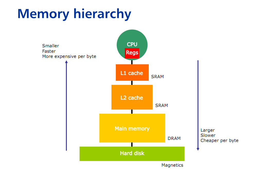
memory hierarchy

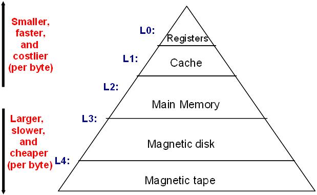
 The term memory hierarchy is used in computer architecture when discussing performance issues in computer architectural design, algorithm predictions, and the lower level programming constructs such as involving locality of reference. A "memory hierarchy" in computer storage distinguishes each level in the "hierarchy" by response time. Since response time, complexity, and capacity are related, the levels may also be distinguished by the controlling technology.
In other word memory hierarchy is the trade off between the cost,capacity and the access time.
The overall goal of using a memory hierarchy in designing the computer system is  to obtain the highest possible average access speed while minimizing total cost of entire memory system.
  • If capacity increases access time increases i.e. slower and due to which cost per bit decreases.
  • If  access time decreases i.e. faster capacity decreases and due to which cost per bit increases. 
It is better to have fastest memory as far a possible to achieve a greater performance ,moreover for  the  practical system the cost must be affective.the designer tries to increases the capacity because cost per bit decreases and the more application ca be accommodated .But at the same time access time increases and hence decreases the performance,
memory hierarchy

memory hierarchy

Memory hierarchy

Memory hierarchy

Types, Construction, Working principle as an amplifier and characteristics of npn Teransistor


he NPN Transistor

In the previous tutorial we saw that the standard Bipolar Transistor or BJT, comes in two basic forms. An NPN (Negative-Positive-Negative) type and a PNP (Positive-Negative-Positive) type, with the most commonly used transistor type being the NPN Transistor. We also learnt that the junctions of the bipolar transistor can be biased in one of three different ways – Common Base, Common Emitter and Common Collector.
In this tutorial about bipolar transistors we will look more closely at the “Common Emitter” configuration using the Bipolar NPN Transistor with an example of the construction of a NPN transistor along with the transistors current flow characteristics is given below.

A Bipolar NPN Transistor Configuration

bipolar npn transistor configuration
(Note: Arrow defines the emitter and conventional current flow, “out” for a Bipolar NPN Transistor.)
 
The construction and terminal voltages for a Bipolar NPN Transistor are shown above. The voltage between the Base and Emitter ( VBE ), is positive at the Base and negative at the Emitter because for an NPN transistor, the Base terminal is always positive with respect to the Emitter. Also the Collector supply voltage is positive with respect to the Emitter ( VCE ). So for a bipolar NPN transistor to conduct the Collector is always more positive with respect to both the Base and the Emitter.
bipolar npn transistor NPN Transistor Connection
Then the voltage sources are connected to an NPN transistor as shown. The Collector is connected to the supply voltage VCC via the load resistor, RL which also acts to limit the maximum current flowing through the device. The Base supply voltage VB is connected to the Base resistor RB, which again is used to limit the maximum Base current.
We know that the transistor is a “current” operated device (Beta model) and that a large current ( Ic ) flows freely through the device between the collector and the emitter terminals when the transistor is switched “fully-ON”. However, this only happens when a small biasing current ( Ib ) is flowing into the base terminal of the transistor at the same time thus allowing the Base to act as a sort of current control input.
The transistor current in a bipolar NPN transistor is the ratio of these two currents ( Ic/Ib ), called the DC Current Gain of the device and is given the symbol of hfe or nowadays Beta, ( β ). The value of β can be large up to 200 for standard transistors, and it is this large ratio between Ic and Ib that makes the bipolar NPN transistor a useful amplifying device when used in its active region as Ib provides the input and Ic provides the output. Note that Beta has no units as it is a ratio.
Also, the current gain of the transistor from the Collector terminal to the Emitter terminal, Ic/Ie, is called Alpha, ( α ), and is a function of the transistor itself (electrons diffusing across the junction). As the emitter current Ie is the sum of a very small base current plus a very large collector current, the value of alpha α, is very close to unity, and for a typical low-power signal transistor this value ranges from about 0.950 to 0.999

α and β Relationship in a NPN Transistor

npn transistor alpha beta relationship
 
By combining the two parameters α and β we can produce two mathematical expressions that gives the relationship between the different currents flowing in the transistor.
transistor alpha and beta relationship
 
The values of Beta vary from about 20 for high current power transistors to well over 1000 for high frequency low power type bipolar transistors. The value of Beta for most standard NPN transistors can be found in the manufactures data sheets but generally range between 50 – 200.
The equation above for Beta can also be re-arranged to make Ic as the subject, and with a zero base current ( Ib = 0 ) the resultant collector current Ic will also be zero, ( β x 0 ). Also when the base current is high the corresponding collector current will also be high resulting in the base current controlling the collector current. One of the most important properties of the Bipolar Junction Transistor is that a small base current can control a much larger collector current. Consider the following example.

NPN Transistor Example No1

A bipolar NPN transistor has a DC current gain, (Beta) value of 200. Calculate the base current Ib required to switch a resistive load of 4mA.
npn transistor base current
 
Therefore, β = 200, Ic = 4mA and Ib = 20µA.
One other point to remember about Bipolar NPN Transistors. The collector voltage, ( Vc ) must be greater and positive with respect to the emitter voltage, ( Ve ) to allow current to flow through the transistor between the collector-emitter junctions. Also, there is a voltage drop between the Base and the Emitter terminal of about 0.7v (one diode volt drop) for silicon devices as the input characteristics of an NPN Transistor are of a forward biased diode.
Then the base voltage, ( Vbe ) of a NPN transistor must be greater than this 0.7V otherwise the transistor will not conduct with the base current given as.
npn transistor base current formula
 
Where:   Ib is the base current, Vb is the base bias voltage, Vbe is the base-emitter volt drop (0.7v) and Rb is the base input resistor. Increasing Ib, Vbe slowly increases to 0.7V but Ic rises exponentially.

NPN Transistor Example No2

An NPN Transistor has a DC base bias voltage, Vb of 10v and an input base resistor, Rb of 100kΩ. What will be the value of the base current into the transistor.
base current calculation
 
Therefore, Ib = 93µA.

The Common Emitter Configuration.

As well as being used as a semiconductor switch to turn load currents “ON” or “OFF” by controlling the Base signal to the transistor in ether its saturation or cut-off regions, Bipolar NPN Transistors can also be used in its active region to produce a circuit which will amplify any small AC signal applied to its Base terminal with the Emitter grounded.
If a suitable DC “biasing” voltage is firstly applied to the transistors Base terminal thus allowing it to always operate within its linear active region, an inverting amplifier circuit called a single stage common emitter amplifier is produced.
One such Common Emitter Amplifier configuration of an NPN transistor is called a Class A Amplifier. A “Class A Amplifier” operation is one where the transistors Base terminal is biased in such a way as to forward bias the Base-emitter junction.
The result is that the transistor is always operating halfway between its cut-off and saturation regions, thereby allowing the transistor amplifier to accurately reproduce the positive and negative halves of any AC input signal superimposed upon this DC biasing voltage.
Without this “Bias Voltage” only one half of the input waveform would be amplified. This common emitter amplifier configuration using an NPN transistor has many applications but is commonly used in audio circuits such as pre-amplifier and power amplifier stages.
With reference to the Common Emitter Configuration shown below, a family of curves known as the Output Characteristics Curves, relates the output collector current, ( Ic ) to the collector voltage, ( Vce ) when different values of Base current, ( Ib ). Output characteristics curves are applied to the transistor for transistors with the same β value.
A DC “Load Line” can also be drawn onto the output characteristics curves to show all the possible operating points when different values of base current are applied. It is necessary to set the initial value of Vce correctly to allow the output voltage to vary both up and down when amplifying AC input signals and this is called setting the operating point or Quiescent Point, Q-point for short and this is shown below.

Single Stage Common Emitter Amplifier Circuit

common emitter amplifier
 

Output Characteristics Curves of a Typical Bipolar Transistor

transistor collector characteristics
 
The most important factor to notice is the effect of Vce upon the collector current Ic when Vce is greater than about 1.0 volts. We can see that Ic is largely unaffected by changes in Vce above this value and instead it is almost entirely controlled by the base current, Ib. When this happens we can say then that the output circuit represents that of a “Constant Current Source”.
It can also be seen from the common emitter circuit above that the emitter current Ie is the sum of the collector current, Ic and the base current, Ib, added together so we can also say that Ie = Ic + Ib for the common emitter (CE) configuration.
By using the output characteristics curves in our example above and also Ohm´s Law, the current flowing through the load resistor, ( RL ), is equal to the collector current, Ic entering the transistor which in turn corresponds to the supply voltage, ( Vcc ) minus the voltage drop between the collector and the emitter terminals, ( Vce ) and is given as:
npn transistor collector current
 
Also, a straight line representing the Dynamic Load Line of the transistor can be drawn directly onto the graph of curves above from the point of “Saturation” ( A ) when Vce = 0 to the point of “Cut-off” ( B ) when Ic = 0 thus giving us the “Operating” or Q-point of the transistor. These two points are joined together by a straight line and any position along this straight line represents the “Active Region” of the transistor. The actual position of the load line on the characteristics curves can be calculated as follows:
npn transistor load line
 
Then, the collector or output characteristics curves for Common Emitter NPN Transistors can be used to predict the Collector current, Ic, when given Vce and the Base current, Ib. A Load Line can also be constructed onto the curves to determine a suitable Operating or Q-point which can be set by adjustment of the base current. The slope of this load line is equal to the reciprocal of the load resistance which is given as: -1/RL
Then we can define a NPN Transistor as being normally “OFF” but a small input current and a small positive voltage at its Base ( B ) relative to its Emitter ( E ) will turn it “ON” allowing a much large Collector-Emitter current to flow. NPN transistors conduct when Vc is much greater than Ve.
In the next tutorial about Bipolar Transistors, we will look at the opposite or complementary form of the NPN Transistor called the PNP Transistor and show that the PNP Transistor has very similar characteristics to the bipolar NPN transistor except that the polarities (or biasing) of the current and voltage directions are reversed.